3D Printed Tungsten Anti Scattering Grid
has great potential in CT scanner
The application potential of 3D printing
(additive manufacturing) tungsten anti scattering grid (ASG) in medical CT
scanner is huge, not only because the high-density metal tungsten has strong
absorption capacity for X-ray scattering, but also because the tungsten
products manufactured with additive have the characteristics of strong
stiffness, thin wall thickness, high density, more absorbed and scattered
radiation and good shading.
CT scanner is one of the ways to diagnose
New Coronavirus pneumonia. With the sudden impact of COVID-19 in 2020, the
market demand for CT equipment increased significantly. As the key component of
CT equipment, the usage of anti scatter grid also increased. The function of
ASG is to absorb and filter the X-rays Scattered, refracted and overflowed from
CT detection, so as to improve the quality of CT image.
ASG is generally made of pure tungsten because it has high requirements for strength, precision, shading, radiation absorption capacity, safety and structural stability. Tungsten is characterized by high melting point, high density, high strength, high thermal conductivity, high hardness, low thermal expansion coefficient and low sputtering erosion rate. Although its good mechanical, thermal and electrical properties make it widely used in medical, military, electronics, aerospace and other fields, it is also because of its high melting point and high hardness that tungsten machining is very difficult.
Generally speaking, from tungsten to the
final product, it needs several deep processing technologies, such as forming,
machining, bonding and surface treatment. However, in the processing process,
tungsten products often appear deformation, crack, creep, stress fracture and
so on, which will reduce their quality.
In order to solve the above problems,
modern manufacturers say that tungsten anti scattering grids can be processed
by selective laser melting process (SLM) in 3D printing technology. SLM
technology selects laser as the energy source and scans the metal powder bed
layer layer by layer according to the path planned in the three-dimensional CAD
slice model. The scanned metal powder achieves the effect of metallurgical
combination through melting and solidification, and finally obtains the metal
parts designed by the model. It not only overcomes the problems brought by
traditional technology in manufacturing metal parts with complex shapes, but
also prepares metal parts with almost full density and good mechanical
properties.
The research shows that the wall thickness
of tungsten anti scattering grid of SLM technology can reach 0.08-0.1mm, the
forming accuracy can be controlled at 0.02mm, and the density can be as high as
99%. Therefore, compared with the products manufactured by traditional
technology, it is more suitable for CT scanners.
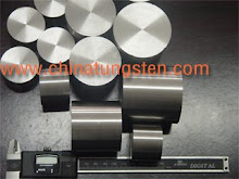
China Tungsten Online has more than 20
years of experience in R & D, producing Tungsten metal and alloy Anti Scattering
Grid by traditional PM method and 3D printed. For more details, please visit our web site www.ctia.com.cn or contact us via sales@chinatungsten.com
没有评论:
发表评论